Privacy Policy Update
Click here to learn about the new Privacy Policy updates from Practical Components.888-388-7808
IP80-0101JY
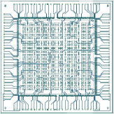
Chip Structure
- Base Layer : P-TEOS*
- Metal Layer : TiN / AI-0.5%Cu
- Passivation Layer : HDP* / P-SiN (option) Polymide
*TEOS : Tetraethoxysilane
*HDP : High Density Plasma
| Specifications | |
| Wafer Size | 8 inch |
| Wafer Thickness | 725±25μm |
| Chip Size | 10.0mm |
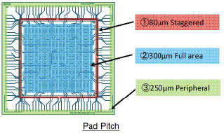
| Pad pitch | 80μm Staggered (Inner pad) 300μm Full area (Center core) 250μm Peripheral (Outer pad) |
| Function | Daisy Chain |
| Pad config | Peripheral and Full Area |
| Pad Size | 58 μm 58 μm 110 μm |
| Passivation opening | 48 μm 48 μm 100 μm |
| Scribe width | 100μm |
| Number of Pad | 648 400 124 |
| Number of Chip | 228 chips/wafer |
| Surface Spec of Electrode | Electroless Ni/Au plating, Al-Si(0.5%) |

Practical Components - Newsletter

Want To Learn More About
Practical Dummy Components?
Sign up for Practical Components e-mails and receive:
* Instant notification of new products and services.
* Special offers only available to our friends.
* Find out about events, get insider tips and more!