Privacy Policy Update
Click here to learn about the new Privacy Policy updates from Practical Components.Flip Chips-Pac Tech Dummy Component



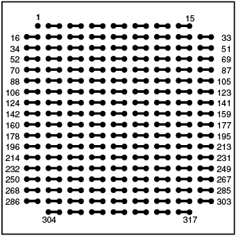


Flip Chips
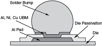
Flip Chip describes the method of electrically connecting the die to the package carrier. The dummy component package carrier, either substrates or leadframe, then provides the connection from the die to the exterior of the package. The interconnection between die and carrier in flip chip packaging is made through a conductive bump that is placed directly on the die surface. The bumped die is then flipped over and placed face down, with the bumps connecting to the carrier. After the die is solderable, underfill is applied between the die and the substrates, around the solder bumps. The underfill is designed to contract the stress in the solder joints caused by the difference in thermal expansion between the silicon die and carrier in this dummy component.
Pac Tech offers a complete set of additional wafer level and backend services including: saw, dice, redistribution, repassivation, backside laser mark, backside coating, test die, and assembly. In addition, Pac Tech has the latest in metrology and analytical equipment to help in the development and production proceses, including: x-ray, shear, AOI, ICP, AA, probing, high speed ball pull, chemical analysis, etc.
|
Flip Chips |
||||||||
|
Part Descriptions |
Die |
No. of Bumps |
Bump |
Bump |
UBM |
Passivation |
UnCut |
Trays |
|
Pac2.3 |
10x10mm |
572 |
200µm/400µm |
75µm |
90µm |
80µm |
"6" Wafer |
36 per Tray |
|
Pac2.5 |
10x10mm |
376 |
100µm |
53µm |
37µm |
27µm |
"6" Wafer |
36 per Tray |
Notes
* * = Die count represents expected yield per wafer.
* All die is packaged in waffle pack trays unless otherwise specified.
* The potential multiple is the number of die repears on the wafer. With the wafer orientated flat down, a right hand coordinate system applies.
* Die Size is from scribe line to center-to-center. Scribe width is 0.05mm Passicated. Each bump is electrically connected to one other bump and isolated form all others to facilitate electrical test.
* Bump pitch is defined as center-to-center distance between passivation openings.
* Bump height is defined as silicon surface to the top of the bump.
* Bump diameter is defined as the maximum diameter.
* UBM = Under Bump Metallurgy
* Unbumped wafers are available upon special request.
* Metal Composition is 5µm Ni, .05µm Au
* Die are packaged in Waffle Packs
* Lead-Free parts available with (SAC305) 96.5%Sn/3.0%Ag/0.5%Cu alloy or (SAC405) 95.5%Sn/4.0%Ag/.05%Cu alloy
* Other Alloys available upon request.
Lead-Free Die
* All Flip Chips are available Lead-Free with (SAC305) 96.5%Sn/3.0%Ag/0.5%Cu or (SAC405) 95.5%Sn/4.0%Ag/0.5%Cu alloys.
*When ordering Lead Free-Flip Chips add "305" or "405" to end of part number.
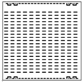
Pac2.3-FA572-200/400-10mm

Die size: 10x10mm (394mils sq)
Pitch: 200µm/400µm (7.88/15.76mil)
Part Description System


About Lead-Free Flip Chips
Flip Chips are used in evaluating assembly techniques, board contiunity, temperature cycle life test evaluation, underfill procsses and other generic needs to be given to the appropriate flux, underfill, temperature profile, and pad finish for the assembly. Many companies are developing and qualifying alternative pad finishes sue as immersion Sn. Lead-Free Flip Chips address the need for environmentally conscious assemblies as well as Alpha particle tolerant packaging.
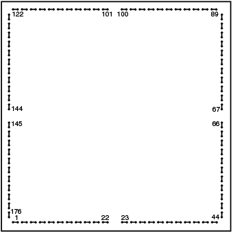
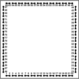
Pac2.5-PB376-100-10mm

Die size: 10x10mm (394mils sq)
Pitch: 100µm (3.94mil)

