Privacy Policy Update
Click here to learn about the new Privacy Policy updates from Practical Components.FA10 Laminate Board

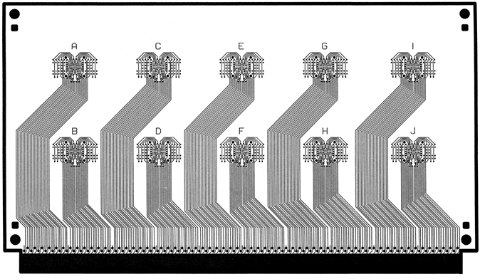
Laminate is only available for FA10-2x2. Single-sided pattern.
Solder practice test vehicle PCB boards and kits are used for machine setup, evaluation, qualification, workflow analysis, prototyping, testing, solder profiling.
Substrate Information
* Board Type—High Temp FR4
* Board Thickness—0.031"
* Layers—4 (top, bottom, ground, power) inner layers nonfunctional
* Copper Conductor—1/4 oz. or 1/2 oz. Cu
* Solder Mask—Taiyo PSR-4000
* Test Site Die—10 (200 x 200 mil2) sites on one side of the board
* Pitch—10?mil array
* Minimum Line—4 mil; Minimum Space—4 mil
* Wettable Cu Pad—5?mil diameter, round
* Through-Hole Via—8 mil drill, 10 mil capture pad
Board for 400x400 die size is not available.
Order Number: FA10-2x2-Laminate
Notes
* Board finish is Organic Solderability Preservative (OSP).OSP, also known as ENTEK® (CU-106A-HT), is a high performance, copper protective coating for use on printed wiring board, which replaces hot air solder leveling (HASL) and other metallic PWB surface finishes. ENTEK® PLUS maintains surface planarity and inhibits copper oxidation. Technical data is on file upon request.
* Digitized files provided by Aegis Software included at no charge.
* Board Size: 3.5" x 5.5"


