Privacy Policy Update
Click here to learn about the new Privacy Policy updates from Practical Components.888-388-7808
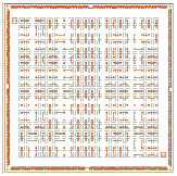
CC80-0101JY
Chip Structure
- Base Layer : P-TEOS*
- Metal Layer : TiN / AI-0.5%Cu
- Passivation Layer : HDP* / P-SiN (option) Polymide
*TEOS : Tetraethoxysilane
*HDP : High Density Plasma
| Specifications | |
| Wafer Size | 8 inch |
| Wafer Thickness | 725±25μm |
| Chip Size | 7.3mm ♦ |
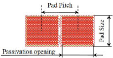
| Pad pitch | 80μm staggered (Peripheral) 300μm Full area (Center core) |
| Function | Daisy Chain |
| Pad config | Peripheral |
| Electrode | Au-stud Bump Wire Bonding Au Plating Cu pillar |
| Pad Size | 58μm ♦ |
| Passivation opening | 48μm ♦ |
| Scribe width | 120μm |
| Number of Chip | 478 chips/wafer |
| ♦ Bottom Side |
| Model | Bump Size | Number of Bumps |
| Model I | ο 38μmor Φ42μm | 1048 *Peripheral (648) / Full Area (400) |
| Model II | ο 38μm | 904 *Peripheral (648) / Full Area (256) |
| Model III | ο 38μm | 728 *Peripheral (648) / Full Area (80) |
| Model IV | ο 38μm | 648 *Peripheral (648) / Full Area (0) |
| *Model IV Compatible to WALTS-TEG MB80-STG0101JY | ||

Practical Components - Newsletter

Want To Learn More About
Practical Dummy Components?
Sign up for Practical Components e-mails and receive:
* Instant notification of new products and services.
* Special offers only available to our friends.
* Find out about events, get insider tips and more!