Privacy Policy Update
Click here to learn about the new Privacy Policy updates from Practical Components.
888-388-7808
Advanced Wafer Technology Substrates
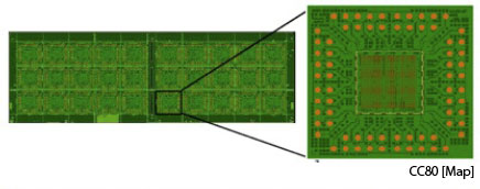
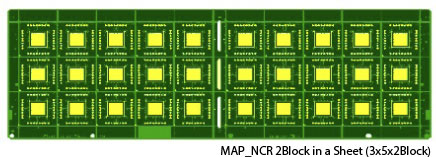
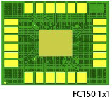
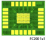
| Part Description | W-Kit-MB50-0102 | W-Kit-CC80-0104 | W-Kit-FC150P-10 | W-Kit-FC200P-10 |
| Specifications | 1x1 | 1x1 | ||
| Structure | 1-2-1 Build Up Substrate | 1-2-1 Build Up Substrate | Rigid Substrate (both) | Rigid Substrate (both) |
| Layer Structure |
Layer 1 Signal Layer (no via) Layer 2 ~ Layer 4 Mesh |
Layer 1,2 Signal Layer (Via) Layer 3, 4 Mesh |
||
| Outline | 17.0mm x 17.0mm x (0.96mmt) |
187.5mm x 64.0mm x (0.36mmt) |
30.0mm x 30.0mm x (0.96mmt) |
30.0mm x 30.0mm x (0.86mmt) |
| Core Material | Core: E-679FGR Build Layer: ABF-GX13 |
Core: E-679FGBS Build Layer: ABF-GX92 |
Core: E-679FGR Build Layer: ABF-GX92 |
Core: E-679FGR |
| Solder Resist Material |
PSR4000 AUS-703 | PSR4000 AUS-703 | PSR4000 AUS-703 | PSR4000 AUS-703 |
| Function | Daisy Chain | Daisy Chain | Daisy Chain | Daisy Chain |
| Land Size | Φ0.12µm | Φ0.14µm | ||
| Lead Min L/S | 20µm/30µm | 32µm/48µm | ||
| Number of Lead |
536 lead | Peripheral: 648 lead Full Area: 400 leads |
3,721 (61x61) | 2,116 (46x46) |
| Pad Dimensions |
Φ0.8µm (SR opening: Φ0.65µm) |
Φ0.75µm (SR opening: Φ0.67µm) |
SR opening: Φ0.80µm | SR opening: Φ0.95µm |
| Number of Pads |
32 Pads | 72 Pads | 24 Pads | 24 Pads |
| Daisy Chain | Center Area 16x15 Matrix Corner Area 15x15 four Matrix |
Center Area 12x12 Matrix Corner Area 12x11 four Matrix |
||
| Surface Spec of Electrode |
Electroless Ni/Au plating | Cu Cu+OSP Electroless Ni/Au plating |
Electroless Ni/Au plating Cu+OSP (Option Solder Coat) Cu |
Electroless Ni/Au plating Cu+OSP (Option Solder Coat) Cu |
| ** Call Practical for custom and option kit substrate options | ||||
Practical Components - Newsletter

Want To Learn More About
Practical Dummy Components?
Sign up for Practical Components e-mails and receive:
* Instant notification of new products and services.
* Special offers only available to our friends.
* Find out about events, get insider tips and more!